
The electronics landscape we inhabit – defined by sleek smartphones, powerful laptops, ubiquitous IoT sensors, and advanced medical devices – would be unimaginable without a silent, foundational revolution: Surface Mount Technology (SMT). While consumers rarely see it, SMT is the invisible engine driving the miniaturization, performance, and affordability of virtually every modern electronic device. It represents a fundamental shift from the bulky, hand-soldered components of the past to the high-speed, precision-engineered manufacturing of today. This article delves deep into the world of SMT, exploring its origins, mechanics, critical equipment, profound advantages, and the cutting-edge trends shaping its future.
From Wires to Whispers: The Genesis of SMT
The story of electronics manufacturing before SMT is one dominated by Through-Hole Technology (THT). Components had long wire leads inserted through drilled holes in the bare Printed Circuit Board (PCB), then soldered, often manually, on the opposite side. While reliable, THT imposed significant limitations:
- Size & Density:Lead holes consumed valuable board real estate, limiting component density and forcing larger PCB sizes.
- Manufacturing Speed:Drilling holes and manual insertion/soldering were slow, labor-intensive processes, ill-suited for mass production.
- Performance:Longer component leads increased parasitic inductance and capacitance, hindering high-frequency circuit performance.
- Automation Difficulty:Automating THT assembly was complex and less efficient.
The seeds of SMT were sown in the 1960s, driven by aerospace and military demands for smaller, lighter, and more reliable electronics. Early "flat packs" and hybrid circuits hinted at the potential. However, it wasn't until the 1980s, fueled by the burgeoning consumer electronics market (especially calculators, watches, and early computers) and crucial advancements in PCB fabrication, component design, and solder paste, that SMT began its ascent from niche to mainstream.
The SMT Process Demystified: A Symphony of Precision
SMT is not a single step but a highly orchestrated sequence of automated processes. Understanding this flow is key to appreciating its sophistication:
1.Solder Paste Application: The process begins with depositing solder paste – a viscous mixture of tiny solder spheres and flux – onto the PCB's designated solder pads. This is primarily done using a Solder Paste Printer and a precision stencil (SMT Stencil or Solder Paste Stencil). The stencil, typically laser-cut stainless steel, aligns perfectly with the PCB. A squeegee blade spreads paste across the stencil, forcing it through apertures and onto the pads below. Precise control of paste volume and alignment is critical here; variations lead to defects like bridging or insufficient solder (Solder Joint Inspection, SPI Machine).

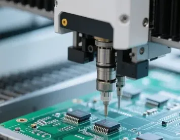
2.Component Placement - The Heartbeat of SMT: This is where speed and precision converge. Pick-and-Place Machines (P&P Machines) are the workhorses. Using sophisticated vision systems, these machines pick miniature components (SMDs - Surface Mount Devices) from reels, trays, or sticks. High-speed rotary heads or gantry systems then place them with incredible accuracy (often within microns) onto the solder-pasted pads. Modern machines handle components ranging from massive connectors down to microscopic 01005 chips (0.4mm x 0.2mm) at staggering speeds of tens of thousands of placements per hour. The type of Pick-and-Place Machine (high-speed, flexible, ultra-precision) is chosen based on production volume and component mix.
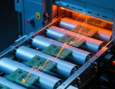
3.Reflow Soldering - Making the Connection: With components tentatively held in place by the paste's tackiness, the PCB travels into a Reflow Oven. This multi-zone oven subjects the assembly to a carefully controlled temperature profile:
- Preheat:Gradually raises temperature to activate flux and evaporate solvents, minimizing thermal shock.
- Soak/Thermal Soak:Allows temperature to equalize across the entire assembly, ensuring flux cleans the metal surfaces.
- Reflow:Temperature peaks (typically 230-250°C for lead-free solder), melting the solder spheres. Surface tension causes the molten solder to wick up component terminations and form a reliable metallurgical bond with the PCB pad – the solder joint.
Cooling:Controlled cooling solidifies the solder joints, completing the electrical and mechanical connection.
Precise control of this profile (Thermal Profiling) is paramount to avoid defects like tombstoning (components standing on end), bridging, cold joints, or component damage.
- Inspection & Quality Control (QC):Post-reflow, assemblies undergo rigorous inspection. Automated Optical Inspection (AOI) systems use cameras to check for missing, misaligned, or wrong components, solder bridging, insufficient/excess solder, and polarity. For complex assemblies or hidden joints (like Ball Grid Arrays - BGAs), X-Ray Inspection (AXI) is used. In-Circuit Test (ICT) and Functional Test (FCT) verify electrical performance. SPI Machines might also be used post-placement to verify paste volume before reflow. This multi-layered QC approach is vital for ensuring reliability.
- Cleaning (Optional):Depending on the flux type used (no-clean, water-soluble, rosin), boards may undergo cleaning to remove flux residues that could cause corrosion or interfere with conformal coating later. Aqueous cleaning systems or specialized solvents are used.
- Conformal Coating (Optional):For electronics exposed to harsh environments (moisture, dust, chemicals), a protective Conformal Coating (acrylic, silicone, urethane, epoxy) is often applied to the assembled PCB (PCBA - Printed Circuit Board Assembly) to insulate and shield components and traces.
Why SMT Reigns Supreme: The Unassailable Advantages
SMT's dominance is no accident. It offers compelling advantages over its THT predecessor:
- Miniaturization & Higher Density:SMDs are inherently smaller and lack long leads. They mount directly onto the board surface, not through This allows for significantly more components in a smaller area, enabling the incredibly compact devices we use daily. High-Density Interconnect (HDI) PCBs, pushing the boundaries of density with microvias and finer traces, are fundamentally reliant on SMT.
- Enhanced Performance:Shorter electrical paths on SMDs reduce unwanted inductance and capacitance, enabling better performance, especially at high frequencies critical for modern computing, telecommunications (5G/6G), and RF applications.
- Improved Reliability:Automated processes minimize human error. Solder joints formed during reflow are generally more consistent and reliable than hand-soldered THT joints. The direct mounting also offers better mechanical stability under vibration.
- Cost-Effectiveness at Scale:While setup costs (stencils, programming) exist, SMT automation drastically reduces labor costs per unit and enables vastly higher production volumes. Reduced PCB size (fewer layers, smaller area) also contributes to cost savings. The efficiency of SMT Lines is unmatched.
- Design Flexibility & Complexity:SMT enables the use of advanced components like BGAs, Quad Flat Packs (QFPs), and Chip-Scale Packages (CSPs) that THT simply cannot accommodate. This allows for far more complex and powerful circuit designs.
- Automation & Speed:The entire SMT process is highly automatable. High-speed Pick-and-Place Machines and continuous Reflow Ovens enable production rates orders of magnitude faster than manual THT assembly, meeting global demand efficiently.
Pushing the Boundaries: Trends Shaping the Future of SMT
SMT is not static; it continuously evolves to meet new challenges and opportunities:
- Extreme Miniaturization (01005, 008004 Components):The relentless drive for smaller devices pushes component sizes down to almost invisible levels (01005: 0.4mm x 0.2mm). This demands ever-higher precision from Pick-and-Place Machines, advanced Solder Paste Stencils with nano-coated surfaces, and sophisticated SPI/AOI systems capable of inspecting these minuscule features.
- Advanced Packaging & Heterogeneous Integration:SMT is adapting to handle not just discrete components, but complex sub-assemblies and advanced packaging techniques:
- System-in-Package (SiP):Integrating multiple chips (processors, memory, RF) and often passive components into a single package, mounted via SMT. This blurs the line between component and board assembly.
- Fan-Out Wafer-Level Packaging (FOWLP):Allows for more I/O connections in a small area than traditional packaging, increasingly handled by advanced placement machines.
- Embedded Components:Passive components (resistors, capacitors) are fabricated within the PCB layers during fabrication, freeing up surface space for active SMDs, further increasing density.
- High-Speed, High-Mix Flexibility:While dedicated high-speed lines exist for volume production, there's a growing need for flexible SMT lines capable of efficiently handling smaller batches with diverse components. Agile Pick-and-Place Machines with quick changeovers and advanced feeders are key.
- Enhanced Process Control & Industry 4.0:Data is king. Integrating sensors throughout the SMT Line (paste printers, placement machines, reflow ovens, inspection systems) allows for real-time monitoring and closed-loop control. AI and machine learning analyze this data to predict and prevent defects, optimize Reflow profiles dynamically, improve yield (First Pass Yield - FPY), and enable predictive maintenance. This "Smart Factory" approach is revolutionizing SMT efficiency and quality.
- Advanced Materials & Soldering Techniques:Demands for higher reliability (automotive, aerospace) and lead-free soldering drive developments in solder paste alloys, fluxes, and PCB materials (high-Tg, low-loss laminates). Techniques like Vacuum Reflow Soldering minimize voids in solder joints under BGAs, crucial for power electronics and high-reliability applications. Selective Soldering is used alongside SMT for the remaining THT connectors or components.
- Sustainability:The industry is focusing on reducing energy consumption in Reflow Ovens, using more environmentally friendly fluxes and cleaning agents, improving recycling of PCBs and components, and designing for disassembly.
SMT: The Indispensable Foundation
It's impossible to overstate SMT's impact. It is the bedrock upon which the modern electronics industry is built. From the simplest consumer gadget to the most complex supercomputer or satellite, SMT enables the production of the sophisticated, miniaturized, and high-performance electronics that define our era. The relentless pace of innovation – demanding ever-smaller, faster, and more powerful devices – ensures that SMT will continue to evolve and remain central to electronics manufacturing for decades to come.
The hum of the Pick-and-Place Machine, the controlled heat of the Reflow Oven, and the meticulous gaze of the AOI system represent more than just a manufacturing process; they represent the quiet, precise heartbeat of our technological world. As trends like SiP, extreme miniaturization, and AI-driven optimization take hold, SMT's silent revolution continues, paving the way for the next generation of electronic marvels. Understanding this technology is fundamental to understanding how our connected, digital future is physically constructed, one precisely placed component at a time.


